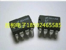
LF353N
- 品牌:
TI
- 封装:
DIP-8
- 数量:
5600
- 备注:
LF353-N SNOSBH3F –APRIL 1998–REVISED MARCH 2013 www.ti.com DC Electrical acteristics LF353-N Symbol Parameter Conditions Units MIn Typ Max VOS Input Offset Voltage RS=10kΩ, TA=25°C 5 10 mV Over Temperature 13 mV ΔVOS/ΔT Average TC of Input Offset Voltage RS=10 kΩ 10 μV/°C IOS Input Offset Current Tj=25°C (1)(2) 25 100 pA Tj≤70°C 4 nA IB Input Bias Current Tj=25°C (1)(2) 50 200 pA Tj≤70°C 8 nA RIN Input Resistance Tj=25°C 1012 Ω AVOL Large Signal Voltage Gain VS=±15V, TA=25°C 25 100 V/mV VO=±10V, RL=2 kΩ Over Temperature 15 V/mV VO Output Voltage Swing VS=±15V, RL=10kΩ ±12 ±13.5 V VCM Input Common-Mode Voltage VS=±15V ±11 +15 V Range 12 V CMRR Common-Mode Rejection Ratio RS≤ 10kΩ 70 100 dB PSRR Supply Voltage Rejection Ratio See(3) 70 100 dB IS Supply Current 3.6 6.5 mA (1) These specifications apply for VS=±15V0°C≤TA≤+70°C. VOS, IBand IOS are measured at VCM=0. (2) The input bias currents are junction leakage currents which approximately double for every 10°C increase in the junction temperature, Tj . Due to the limited production test time, the input bias currents measured are correlated to junction temperature. In normal operation the junction temperature rises above the ambient temperature as a result of internal power dissipation, PD. Tj=TA+θjA PD where θjA is the thermal resistance from junction to ambient. Use of a heat sink is recommended if input bias current is to be kept to a minimum. (3) Supply voltage rejection ratio is measured for both supply magnitudes increasingdecreasing simultaneously in accordance with
- 批号:
2021+
- 价格:


